[color=rgb(51, 51, 51) !important]电子元器件的等效电路对电路分析非常有用,可以帮助理解该元器件在电路中的工作原理,可以深入了解该元器件的相关特性。
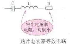
* P+ c. N+ Q9 y0 O' Z[color=rgb(51, 51, 51) !important]贴片电容器等效电路
7 j/ g% q) E, S( `' A[color=rgb(51, 51, 51) !important]下图所示是贴片电容器的等效电路。
[color=rgb(51, 51, 51) !important]从等效电路可以看出,电容器除电容外还有寄生电感L和寄生电阻R,尽管L值和R值都很小,但是在工作频率很高时电感会起作用,电感L与电容C构成一个LC串联谐振电路。
l$ \" w; G: e1 _ z[color=rgb(51, 51, 51) !important]有引脚电容器等效电路
[color=rgb(51, 51, 51) !important]下图所示是有引脚电容器的等效电路。
0 y, k/ V. {: i. L% Z- S9 H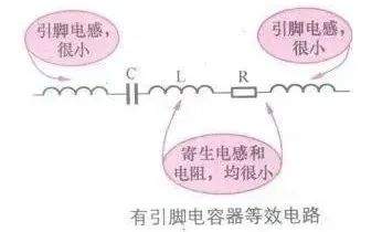
[color=rgb(51, 51, 51) !important]它与贴片电容器相比,其等效电路中多了引脚分布电感,它也有高频串联谐振的特性。
9 T* @ S* f/ f6 h. J/ i2 H[color=rgb(51, 51, 51) !important]有极性电解电容等效电路
[color=rgb(51, 51, 51) !important]下图所示是有极性电解电容器的等效电路,这是没有考虑引脚分布参数时的等效电路。
/ ^. z8 Q+ w3 n; A. ]8 \( I$ I4 `: }' K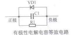
[color=rgb(51, 51, 51) !important]等效电路中,C1位电容,R1为两电极之间的漏电阻,VD1为具有单向导通特性的氧化膜。
[color=rgb(51, 51, 51) !important]大容量电解电容器等效电路
[color=rgb(51, 51, 51) !important]电解电容器是一种低频电容器,即它主要工作在频率较低的电路中,不宜工作在频率较高的电路中,因为电解电容器的高频特性不好,容量很大的电解电容器其高频特新更差。下图所示是大容量电解电容器等效电路,从图中可以找到大容量电解电容器高频特性差的原因。
k% _ D+ P; L5 {" M8 |* u/ b }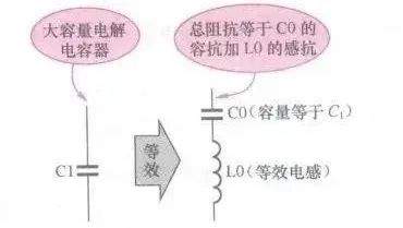
[color=rgb(51, 51, 51) !important]从等效电路中可以看出,串连一只等效电感L0,当电解电容的容量越大时,等效电感L0也越大,高频特性越差。
[color=rgb(51, 51, 51) !important]普通晶闸管等效电路
[color=rgb(51, 51, 51) !important]下图所示是普通晶闸管结构示意图和等效电路。
! ^5 N- Y! d. F6 |7 ?$ v' R9 P" p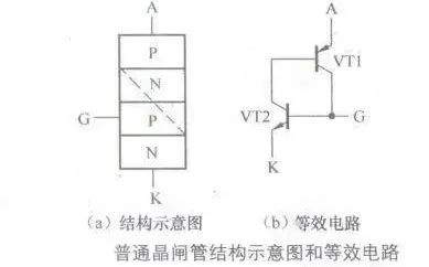
[color=rgb(51, 51, 51) !important]从等效电路中可以看出,普通晶闸管相当于两只三极管进行一定方式的连接后的电路。
) G7 ?4 v5 m; Z* T% [[color=rgb(51, 51, 51) !important]双向晶闸管等效电路
( i! j, Y3 E* P6 n" Z[color=rgb(51, 51, 51) !important]下图所示是双向晶闸管结构示意图和等效电路。
U1 s3 @6 W4 }/ U1 h! M$ b3 i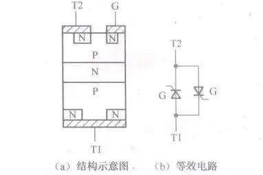
[color=rgb(51, 51, 51) !important]从等效电路中可以看出,双向晶闸管相当于两只普通晶闸管反向并联。
7 f3 M6 ^- y" ]$ z& C[color=rgb(51, 51, 51) !important]四极晶闸管等效电路
[color=rgb(51, 51, 51) !important]下图所示是四极晶闸管结构示意图和等效电路。
" Q" }; B/ }/ @5 L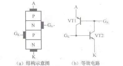
[color=rgb(51, 51, 51) !important]逆导晶闸管的等效电路
[color=rgb(51, 51, 51) !important]下图所示是逆导晶闸管的等效电路。
( r+ a. r- B a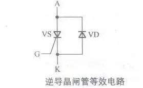
[color=rgb(51, 51, 51) !important]从等效电路中可以看出,逆导晶闸管相当于在普通晶闸管上反向并联一只二极管。
I7 K0 N" Z5 m7 @' t: v3 {[color=rgb(51, 51, 51) !important]BTG晶闸管等效电路
[color=rgb(51, 51, 51) !important]下图所示是BTG晶闸管结构示意图和等效电路。
$ C5 | |( R! g8 ^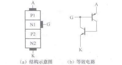
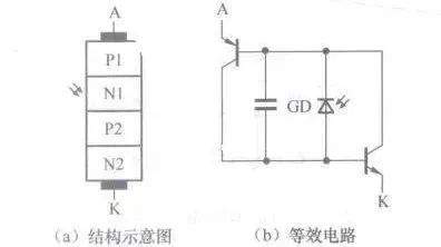
[color=rgb(51, 51, 51) !important]光控晶闸管等效电路
[color=rgb(51, 51, 51) !important]下图所示是光控晶闸管结构示意图和等效电路。
[color=rgb(51, 51, 51) !important]电阻器的等效电路
7 M M! S, z* S: O[color=rgb(51, 51, 51) !important]下图所示为电阻器的等效电路。等效电路中,R为标称电阻器,L为分布电感,C为分布电容。由于分布电感L和分布电容C均很小,所以当电阻器的工作频率不是很高时,它们的影响都可以不考虑。
' l- `; X& y2 i# j9 M% ?: ?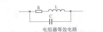
[color=rgb(51, 51, 51) !important]在工作频率很高的电路中,应该使用高频电阻器,它们的分布电感L和分布电容C比普通电阻器的更小。
[color=rgb(51, 51, 51) !important]压敏电阻器等效电路
[color=rgb(51, 51, 51) !important]下图所示是压敏电阻器等效电路。等效电路中,Rn是晶界电阻,C是晶界电容,Rb是晶粒电阻。
% M; ]" @* E7 ?1 J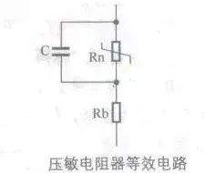
[color=rgb(51, 51, 51) !important]下图是压敏电阻器伏-安特性曲线中的3个工作区示意图,它的3个工作区包括预击穿区、击穿区和上升区。

[color=rgb(51, 51, 51) !important]电感器等效电路
[color=rgb(51, 51, 51) !important]电感器固有电容又称为分布电容和寄生电容,它是由各种因素造成的,相当于并联在电感线圈两端的一个总的等效电容。下图所示是电感器等效电路,电容C为电感器的固有电容,R为线圈的直流电阻,L为电感。
9 B) o' @6 W+ l# p& _1 l% a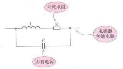
[color=rgb(51, 51, 51) !important]电感L与等效电容C构成一个LC并联谐振电路,这一电路将影响电感器的有效电感量的稳定性。当电感器工作在高频电路中时,由于频率高,容抗小,所以等效电容对电路工作影响大,为此要尽量减小电感线圈的固有电容。当电感器工作在低频电路中时,由于等效电容的容量很小,工作频率低时它的容抗很大,故相当于开路,所以对电路工作影响不大。不同应用场合对电感器不同参数的要求是不同的,只有了解了这些参数的具体含义,才能正确使用这些参数。
[color=rgb(51, 51, 51) !important]变容二极管等效电路
! O+ _; G1 L D+ b) y }$ z[color=rgb(51, 51, 51) !important]下图所示是变容二极管等效电路。

[color=rgb(51, 51, 51) !important]等效电路中的C为可变结电容,它可近似看成为变容二极管的总电容,它包括结电容、外壳电容及其它分布电容。R是串联电阻,它包括PN结电阻、引线电阻及接线电阻;L是引线电感。
[color=rgb(51, 51, 51) !important]双向触发二极管等效电路
[color=rgb(51, 51, 51) !important]下图所示是双向触发二极管结构示意图和等效电路。
4 x e2 ]9 r- O) ~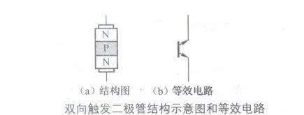
[color=rgb(51, 51, 51) !important]石英晶振等效电路
[color=rgb(51, 51, 51) !important]下图所示是石英晶振等效电路。从等效电路中可以看出,石英晶振相当于一个LC串联谐振电路。
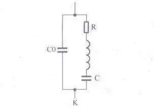
[color=rgb(51, 51, 51) !important]陶瓷滤波器等效电路
[color=rgb(51, 51, 51) !important]图所示是陶瓷滤波器等效电路。陶瓷滤波器由1个或多个压电振子组成,双端陶瓷滤波器等效为一个LC串联谐振电路。由LC串联谐振电路特性可知,谐振时该电路的阻抗最小,且为纯阻性。不同场合下使用的双端陶瓷滤波器的谐振频率不同。
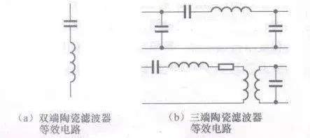
[color=rgb(51, 51, 51) !important]三端陶瓷滤波器相当于一个双调谐中频变压器,故比双端陶瓷滤波器的滤波性能要更好些。
4 w/ R9 s8 O4 _% m: w' f" k, {" ^[color=rgb(51, 51, 51) !important]普通复合管(达林顿管)内电路
[color=rgb(51, 51, 51) !important]复合管电路共有4种。复合管用两只三极管按一定方式连接起来,等效成1只三极管,下图所示是4种复合管等效电路。
- f4 @) I& z. c5 [& b+ r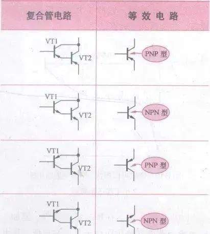
[color=rgb(51, 51, 51) !important]复合管极性识别绝招:2只三极管复合后的极性取决于第1只三极管的极性。
[color=rgb(51, 51, 51) !important]大功率复合管内电路
# p% \7 w) A8 |[color=rgb(51, 51, 51) !important]下图所示是2种大功率复合管内电路。从内部电路中可以看出,它设有过电压保护电路(采用稳压二极管)。
* C% E: j$ T1 y' d. {3 z* Q$ N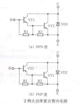
[color=rgb(51, 51, 51) !important]带阻尼的行管等效电路
6 M; P d, \+ K- W0 E[color=rgb(51, 51, 51) !important]下图所示是带阻尼的行管电路符号和等效电路。
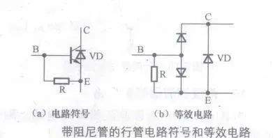
[color=rgb(51, 51, 51) !important]行输出级电路中需要一只阻尼二极管,在一些行输出三极管内部设置了这一阻尼二极管,在行输出管的电路符号中会表示出来。这种三极管内部在基级和发射极之间还接入1只25欧姆的小电阻R0。将阻尼二极管设在行输出管的内部,减小了引线电阻,有利于改善行扫描线性和减小行频干扰,基级与发射极之间接入的电阻是为了适应行输出管工作在高反向耐压的状态。
5 O( t* r2 J9 J0 }0 ?4 ?& V) N| 欢迎光临 EDA365电子论坛网 (https://bbs.eda365.com/) | Powered by Discuz! X3.2 |